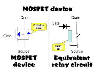
First of all I will explain the nMos type, nMos types are considered to be a voltage-controlled switch, meaning that there is a Voltage source supplied to the drain terminal and an earth is supplied to the source terminal, these terminals are not joined, so how do we allow current flow? this is where our gate terminal comes in. (As you can see the mosfet was designed to suit electron flow, not conventional flow). The gate terminal is also supplied with a voltage, but this is for a different reason, not to supply voltage to a consumer. By supplying voltage to our gate terminal basically we allow the MOSFET to bridge the gap between drain and source. How does it do this? Well, this transistor has a compound built in;
 As you can see in this diagram above, the compound involved in this particular MOSFETs body is made up of a p type material(the blue region in this diagram) this is usually made of Si02(silicon oxide) earlier transistors used a metal compound.
When enough voltage is supplied to the gate terminal, the electrons will break through the resistance between the gate and the material forming a bridge from drain to source, thus allowing current flow.
Here is a quick video displaying how a MOSFET works;
pMos transistors work in pretty much the same way, except for the compound construction etc etc, the best way for me to describe how a pMos transistor works is to show a video;
So that pretty much shows how a pMos transistor works, very similar to the nMos transistor, except instead of having a bridge between source and drain, little holes open up allowing current flow.
Referencing;
pmos video http://www.youtube.com/watch?v=9X2YneHJR9g
MOSFET video http://www.youtube.com/watch?v=v7J_snw0Eng
All the pictures found were supplied by googles image search
All info was produced by research of the 4847 workbook and wikipedia
